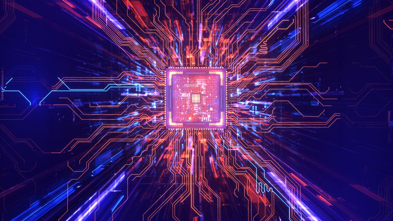
Scientists use quantum machine learning to create semiconductors for the first time – and it could transform how chips are made

Micro -crosses feed almost all modern devices – phones, laptops and even refrigerators. But behind the scenes, make a complex process. But the researchers say that they have found a way to draw from the power of quantum computers to simplify it.
Australian scientists have developed a quantum automatic learning technique – a mixture of artificial intelligence (Ai) and quantum calculation Principles – which could change the way the firms are made.
They described their results in a new study published on June 23 in the journal Advanced science. In this document, researchers have demonstrated for the first time how quantum automatic learning algorithms can significantly improve the difficult process of modeling electrical resistance inside a chip – a key factor that affects its effective workforce.
Quantum automatic learning is a hybrid approach that combines conventional data with quantum calculation methods. In classic IT, data is stored in bits coded in 0 or 1.. Quantum computers use qubits and, thanks to principles such as overlapping and tangle, qubits can exist simultaneously in several states – so that two qubits can be simultaneous at 00, 01, 10 and 11.
This allows quantum IT systems to deal with complex mathematical relationships much faster than conventional systems – with a parallel treatment in the scale exponentially, the more qubits you add to a system
Quantum automatic learning takes conventional data and code in quantum states. The quantum computer can then discover models in data that would be difficult to detect for conventional systems. A classic system then takes over to interpret the results or apply them.
In relation: The “Quantum Ai” algorithms already exceed the fastest supervisors, says the study
Inside the flea manufacturing process
The manufacture of semiconductors is a complex process with several steps which requires meticulous precision – and each step must be carried out with extreme precision. Even the smallest disaling down can make a chip fail.
This first implies the stack and the sculpture often hundreds of microscopic layers on a sliced silicon – a thin slice of circular silicon which forms the foundation of the chip.
Deposit layers of thin materials of material on the edge. The photoresistor coating applies a material sensitive to light which allows precise structuring – the process of creating the tiny complex forms which define the circuits of a chip.
In lithography, light transfers these patterns to the surface of the slice. The engraving then eliminates the selected material zones to carve out circuit structures. Ionic location adjusts the electrical properties of each layer by incorporating loaded particles. Finally, the chip is excited, which means that it is locked up and connected so that it can be integrated into a device.
This is where quantum IT principles come into play. In the study, researchers focused on modeling resistance to ohmic contacts – a particularly difficult challenge in the manufacture of tokens. This is a measure of the ease with which electricity circulates between the metallic and semiconductor layers of a chip; The lower it is, the faster and more energy efficient performance can be.
This step occurs after the materials are in layers and motivated on the edge, and it plays an essential role in determining the way in which the finished chip will work. But precisely modeling it was a problem.
Engineers generally count on conventional automatic learning algorithms, which learn data models to make predictions, for this type of calculation. Although it works well with large sets of clean data, semiconductor experiences often produce small, noisy data sets with non-linear models, where automatic learning can fail. To remedy this, the researchers turned to quantum automatic learning.
A new type of algorithm
The team worked with data from 159 experimental transistor samples with high electron electron (GAN HEMTS) – semiconductor known for their speed and efficiency, commonly used in electronics and 5G devices.
First of all, they identified the manufacturing variables had the greatest impact on resistance to ohmic contacts, narrowing the data set with the most relevant inputs. Then, they developed a new automatic learning architecture called regressor aligned with the quantum nucleus (QKAR).
QKAR converts conventional data into quantum states, allowing the quantum system to then identify complex relationships in the data. A classic algorithm then learns from these ideas, creating a predictive model to guide the manufacture of fleas. They tested the model on five new samples which were not included in the training data.
The new model was tested on these samples against seven classic leading models, in particular in -depth learning and the reinforcement methods of the gradient and that has surpassed them. QKAR obtained a significantly better result than what is obtained using traditional models (0.338 ohm per millimeter) – although specific figures were not included in the study.
Above all, however, it was designed to be compatible with the material of the real world, which means that it could be deployed on quantum machines because they become more reliable.
“These results demonstrate the potential of [quantum machine learning] QML to effectively manage small regression tasks in semiconductor fields, “wrote scientists in the study. They added that the method could soon be applied to the production of real fleas, especially since quantum material continues to evolve.


